

Indian American Contributes To Trickle-down Method to 'Grow' Graphene
Past making carbon leak (trickle downwardly) through cracks on copper, researchers have adult a new process for "growing" graphene directly on materials used for nano-scale electronic applications, thereby opening the way to produce high-functioning electronic devices.
This versatile process, developed past a team of chemic engineers led by Indian-American Vikas Berry at the Academy of Illinois at Chicago (UIC) in the U.s.a., enables graphene to be economically grown on about any semiconducting or dielectric substrate of relevance to the electronic industry, the researchers claim.
They have reported this new method in the journal "ACS Applied Materials and Interfaces" of the American Chemical Club and have obtained two US patents.
"This method can be a game-changer for applications of the wonder textile graphene," Sanjay Behura, research assistant professor at UIC and one of the authors, told IANS in an e-mail.
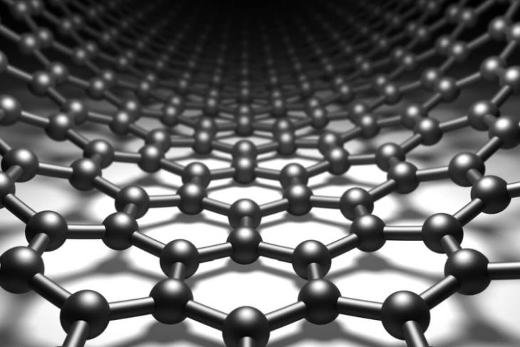
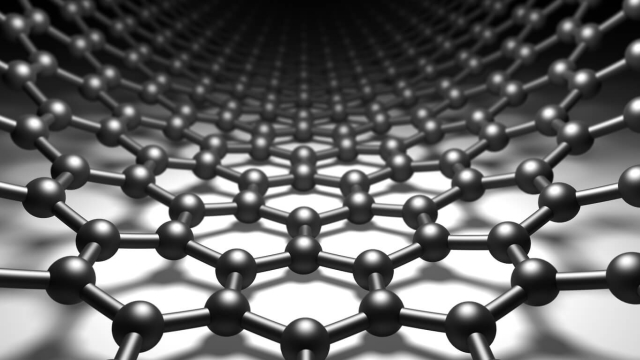
Discovered in 2004, graphene is a sheet of a unmarried layer of carbon atoms, bundled in a ii-dimensional honeycomb lattice.
Due to the ultrafast mobility of its charge carriers, graphene has shown hope in nanoelectronics, optoelectronics and photonics. It besides possesses a plethora of extraordinary mechanical and thermal properties that are nevertheless beingness exploited.
For nanoelectronic device fabrications, it is essential to transfer the graphene — grown separately on metallic substrates — onto selected dielectric substrates.
Current techniques used in the transfer involve a contamination-prone process that introduces unwanted defects and impurities in graphene, making it unfavourable for high-performance nano and optoelectronic devices and industrial applications.
The researchers have overcome this problem by developing a process called "Grain Boundary-Diffusion of Carbon Radicals" for growing high-quality graphene directly on the dielectric substrates, eliminating the need for the contamination-prone transfer procedure.
This "direct" process involves dissociation of methane (carbon source) in a heated furnace in vacuum. The carbon radicals thus produced from methane dissociation lengthened (trickle) through the grain boundaries of polycrystalline copper thin pic and crystallize into graphene at the interface of copper and silicon-based dielectric substrates.
This strategy of growing graphene directly on the substrates is suitable to produce large-scale graphene for industrial applications ranging from nanoscale electronics to energy conversion and optoelectronics, the authors study.
Other contributors of this work include Phong Nguyen from Air Liquide and Michael Seacrist from SunEdison Semiconductors.

Source: https://beebom.com/indian-american-contributes-to-trickle-down-method-to-grow-graphene/
Posted by: conedade1956.blogspot.com
0 Response to "Indian American Contributes To Trickle-down Method to 'Grow' Graphene"
Post a Comment